

Have you ever wondered what lies beneath the sleek surface of your smartphone or the intricate circuitry of your computer?
Hidden within these technological marvels are the secrets of perfect crystals in semiconductor metallurgy.
These flawless structures, meticulously engineered at the atomic level, hold the key to unlocking the full potential of our electronic devices.
But how do we achieve perfection in a world filled with imperfections?
Can we truly harness the power of these flawless crystals, or are we forever bound by the limitations of our materials?
Join me on a journey into the fascinating realm of perfect crystals, where science and innovation collide to shape the future of technology.

What is Semiconductor Metallurgy?
Semiconductor metallurgy is a branch of metallurgy that deals with the production and processing of semiconductors. Semiconductors are materials that have electrical conductivity between that of a conductor and an insulator.
In semiconductor metallurgy, high-purity raw materials like silicon are used, and controlled amounts of impurities called dopants are added to modify the electronic properties of the material.
How does it work?
In semiconductor metallurgy, perfect crystals play a crucial role. Perfect crystals are highly ordered and defect-free crystals with a uniform arrangement of atoms or molecules. They have unique mechanical and optical properties that make them useful for high-quality optoelectronic devices.
The conductivity of semiconductors can be modified by introducing impurities into their crystal lattice, a process known as doping.
Perfect crystals are important because they can be doped to create semiconductors with specific electrical properties.
Methods of Forming Perfect Crystals
There are several methods used in semiconductor metallurgy to form perfect crystals:
Czochralski method
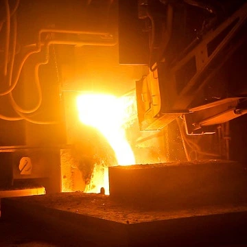
The Czochralski method is a common technique used to produce single crystals of semiconductors like silicon. In this method, high-purity semiconductor-grade silicon is melted in a crucible at a high temperature.
A seed crystal is then dipped into the molten silicon and slowly pulled out.
As the seed crystal is withdrawn, the silicon solidifies around it, forming a single crystal.
Excitonic crystal growth
Excitonic crystal growth is a method used to grow perfect and contamination-free crystals of semiconductors like gallium phosphide (GaP). This method involves the use of a high-temperature furnace and a source of high-purity GaP.
The GaP is heated to a high temperature and allowed to cool slowly, resulting in the formation of a perfect crystal.
Crystal engineering
Crystal engineering is a method of synthesizing functional crystalline solids by controlling the crystal structure. It involves the use of organic optoelectronic materials and can be used to engineer perfect crystals of semiconductors.
Intrinsic defects in semiconductors
Intrinsic defects, such as dislocations, can form closed dislocation loops within a crystalline solid, resulting in the formation of perfect crystals.
Impact of Perfect Crystals on Semiconductor Devices
Perfect crystals have a significant impact on the performance and efficiency of semiconductor devices. Here are some ways in which perfect crystals affect semiconductor devices:
- Perfect crystals have a uniform and regular atomic structure, allowing for better control of the electrical properties of the semiconductor material.
- Perfect crystals have fewer crystal defects, such as dislocations and stacking faults, which can negatively affect the electrical properties of the semiconductor material.
- Perfect crystals have a higher carrier mobility, meaning that electrons and holes can move more easily through the material, resulting in faster and more efficient electronic devices.
- Perfect crystals have a higher thermal conductivity, allowing them to dissipate heat more efficiently, resulting in better thermal management of electronic devices.
Challenges in Achieving Perfect Crystals
Achieving perfect crystals in semiconductor metallurgy is a challenging task due to various limitations and challenges. Some of these challenges include:
- Presence of impurities: It is impossible to obtain any substance in 100% pure form, and some impurities are always present. Cooling the liquid phase too quickly can result in trapped impurities or imperfect alignment of the lattice.
- External stress: Applying external stress to a crystal can cause microscopic regions of the lattice to move, resulting in imperfect alignment.
- Characterization of imperfections: Distinguishing between different types of defects in crystals is a challenging task.
- Growth conditions: Even small variations in the growth conditions can lead to the formation of defects and impurities in crystals.
- Measurement of crystal phase: Measuring the crystal phase remains challenging, requiring high-throughput methods like powder X-ray diffraction and electron diffraction.
Despite these challenges, researchers are continuously working on developing new techniques and methods to overcome them and achieve near-perfect crystals in semiconductor metallurgy.
Analysis and Evaluation of Perfect Crystals
Several techniques and methods are used to analyze and evaluate perfect crystals in semiconductor metallurgy. Some of these techniques include:
- Czochralski method: This crystal growth method is used to obtain single crystals of semiconductors like silicon. It involves melting high-purity silicon in a crucible and adding dopant impurity atoms to dope the silicon, changing its electronic properties.
- Float-zone crystal growth technique: This method is used to grow single crystal silicon for semiconductor applications. It involves passing a rod of silicon through a high-frequency induction coil, melting a small zone of the rod, and allowing a single crystal to grow behind it.
- Oxygen strengthening: Oxygen can be used to mechanically strengthen silicon crystals and provide a means for gettering unwanted impurities.
- Zone melting and crystal growing: This technique involves several methods of zone melting and crystal growing, used to purify and grow crystals of various materials, including semiconductors.
- Doping: The process of adding controlled impurities to a semiconductor is known as doping. The amount and type of impurity added to a pure semiconductor vary its level of conductivity.
The quality of perfect crystals heavily influences the overall quality and reliability of semiconductor devices. Perfect crystals are used in various industries and applications, including the electronics industry, optoelectronics industry, turbine blade production, and colloidal nanocrystals.
Ongoing Research and Advancements
Ongoing research in the field of perfect crystals in semiconductor metallurgy focuses on creating materials with high optical transparency, high electrical conductivity, and high mechanical flexibility.
Some recent advancements include:
- Major advances in semiconductor materials, creating crystals with high optical transparency, high electrical conductivity, and high mechanical flexibility.
- Controlling light emitted by exotic crystal semiconductors, leading to more efficient solar cells.
- Research on 'perfect crystals' and their potential for technical innovation.
- Advances in metallurgy and properties of superalloys, improving the cyclic oxidation resistance of turbine blades.
- Research on single crystal silicon, widely used as a substrate material in semiconductor applications.
- Discovering the most efficient semiconductor by aligning tungsten diselenide crystals with sapphire crystals.
These advancements have the potential to lead to more efficient solar cells, better electronic devices, and other technical innovations in the field of semiconductor metallurgy.

Final analysis and implications
So, we've been diving deep into the fascinating world of semiconductor metallurgy, exploring the concept of perfect crystals. And let me tell you, it's been quite a mind-boggling journey. We've uncovered the intricate structures and properties of these flawless arrangements of atoms, and it's left me with more questions than answers.
Imagine a crystal so perfect that every atom is perfectly aligned, forming a flawless lattice structure. It's like a symphony of atoms, each playing their part in perfect harmony. These perfect crystals possess extraordinary properties, making them ideal for various applications in the semiconductor industry. But here's the thing that keeps me up at night: can perfection truly exist in our imperfect world?
We strive for perfection in so many aspects of our lives, from our work to our relationships. But is perfection just an illusion, a mirage that we chase endlessly? In the realm of semiconductor metallurgy, perfect crystals seem to defy the very nature of our universe. They challenge our understanding of imperfection and make us question the limits of what is possible.
But perhaps, in this pursuit of perfection, we are missing out on something truly remarkable. Imperfections, after all, can be beautiful in their own right. Think about a diamond, with its unique flaws and inclusions. It's these imperfections that give it character and make it one-of-a-kind. Maybe, just maybe, the same can be said for the crystals in semiconductor metallurgy.
What if imperfections in crystals could lead to new discoveries and breakthroughs? What if these flaws hold the key to unlocking even greater potential? It's a thought that both excites and confusees me. Maybe, in our quest for perfection, we should embrace the imperfections and see where they take us.
So, as we wrap up this exploration of perfect crystals in semiconductor metallurgy, I leave you with this food for thought: perfection may be an enticing goal, but it's the imperfections that make life interesting. Embrace the flaws, challenge the boundaries, and who knows what extraordinary possibilities may lie ahead.
Links and references
- Semiconductor crystals
- The Materials Science of Semiconductors
- Applications of phase diagrams in metallurgy and ceramics Volume 1
- The Modelling of Dislocations in Semiconductor Crystals
- Discovering Crystal Forms of the Novel Molecular Semiconductor OEG-BTBT
- Semiconductor Devices
My article on the topic:
What is a perfect crystal and why they don't exist?
Do you know anyone who has been studying and could also benefit from this material?
Share on…
